
Influence of light pattern thickness on the manipulation of dielectric microparticles by optoelectronic tweezers


Published on 2024/08/20 Research powered by Mightex’s Polygon1000 ![]()
 Zhang, S., Elsayed, M., Peng, R., Chen, Y., Zhang, Y., Neale, S. L., & Wheeler, A. R., Influence of light pattern thickness on the manipulation of dielectric microparticles by optoelectronic tweezers, Photonics Research, 10(2), 550-556 (2022).


Introduction
Optoelectronic tweezers (OET) are a micromanipulation technology that uses optically induced dielectrophoresis (ODEP) forces to control micro- and nano-scale objects [1, 2]. By utilising light-patterned electric fields, OET can exert precise pico-to-nano Newton forces, making it effective for manipulating multiple objects simultaneously. This technology has been applied in various fields, including manipulation and assembly of bio-analytes and molecules, cell manipulation, and microrobot control, and has been adopted in the biopharmaceutical industry for antibody discovery and cell therapy [3-5].
Previous studies have shown that the wavelength and intensity of light can be used to control the moving behavior of the micro-objects [6, 7]. While it’s more difficult to change the wavelength and intensity when using a fixed light source, in this study, the researchers focus on a more adjustable factor – the width or thickness of the projected light pattern.

Figure 1: a) Schematic of an OET device, in which microparticles are manipulated via positive or negative DEP forces. b) Video frame showing the use of dynamic light patterns projected from Mightex Polygon DMD device to rotate polystyrene microbeads. Red and yellow arrows represent the counterclockwise and clockwise rotation of beads in the central and surrounding regions respectively.
Methods and Results
The OET setup utilised a Mightex Polygon1000 digital micromirror device (DMD) with a 625 nm LED source, interfaced with a Nikon Eclipse Ni-E microscope, motorised stage, and CMOS camera.
The OET devices comprised a 20 μL fluidic chamber between two glass plates with a 150 μm spacer. The plates were coated with indium tin oxide (ITO) and an additional 1 μm layer of a-Si:H coating on the bottom plate. The system was driven by a 10 Vpp, 20 kHz square wave AC potential from a function generator and amplifier, which creates a non-uniform electric field in the liquid microchamber and on interaction with micro-object, creates DEP forces. Depending on the polarizability of the micro-object in comparison to the surrounding medium, it can be attracted to the illuminated region (positive DEP forces) or repelled by the illuminated region (negative DEP forces)
Zhang et al used 10μm Polystyrene microparticle suspensions prepared in deionized water containing Tween 20 (0.05% volume fraction) before loading into the OET devices. To study how light pattern thickness affects microparticle movement, a single 10-μm-diameter bead was trapped using “doughnut”-shaped light patterns with varying ring thicknesses (2.5 to 135 μm). The light pattern was kept stationary while moving the motorized stage linearly, causing the bead to move in the opposite direction. The bead’s velocity, which equilibrated due to viscous drag and DEP forces, was measured as the stage speed increased.
Video: Different thickness of light patterns can be used to move a microbead at different speeds.
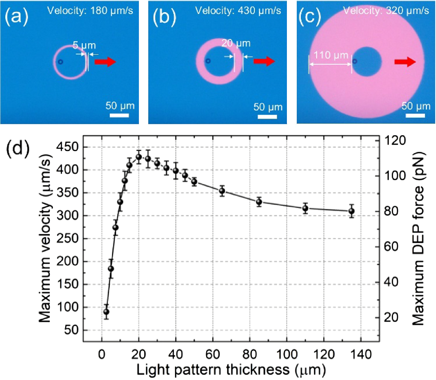
Figure 2: (a)–(c) Images of a microbead trapped by doughnut-shaped light patterns of different ring thicknesses. (d) Maximum velocity and maximum DEP force versus light pattern’s ring thickness.
The maximum velocity of the bead increased with light pattern thickness up to 20 μm, after which it slightly decreased. This behavior was linked to DEP forces, which ranged from about 20 pN to over 100 pN, peaking with a 20 μm thickness. Beyond this, the increase in vertical DEP forces at larger thicknesses (e.g., 135 μm) caused the bead to escape the trap more easily, resulting in a velocity saturation around 300 μm/s.
References:
1. P.Y. Chiou, A.T. Ohta, and M.C. Wu, “Massively parallel manipulation of single cells and microparticles using optical images.” Nature 436, 370-372 (2005).
2. M. Woerdemann, C. Alpmann, M. Esseling, and C. Denz, “Advanced optical trapping by complex beam shaping.” Laser Photon. Rev. 7, 839-854 (2013).
3. S. Zhang et al., “The optoelectronic microrobot: a versatile toolbox for micromanipulation.” Proc. Natl. Acad. Sci. USA 116, 14823-14828 (2019).
4. D. Han and J.K. Park, “Optoelectrofluidic enhanced immunoreaction based on optically-induced dynamic AC electroosmosis.” Lab Chip 16, 1189-1196 (2016).
5. Y.H. Lin, C.M. Chang, and G.B. Lee, “Manipulation of single DNA molecules by using optically projected images.” Opt. Express 17, 15318-15329 (2009).
6. W. Liang, S. Wang, Z. Dong, G.B. Lee, and W.J. Li, “ Optical spectrum and electric field waveform dependent optically induced dielectrophoretic (ODEP) micromanipulation.” Micromachines 3, 492-508 (2012).
7. J.K. Valley et al., “Operational regimes and physics present in optoelectronic tweezers.” J. Microelectromech. Cyst. 17 342-350 (2008).
Megha Patwa, Applications Specialist at Mightex
To read the full publication, please click here.